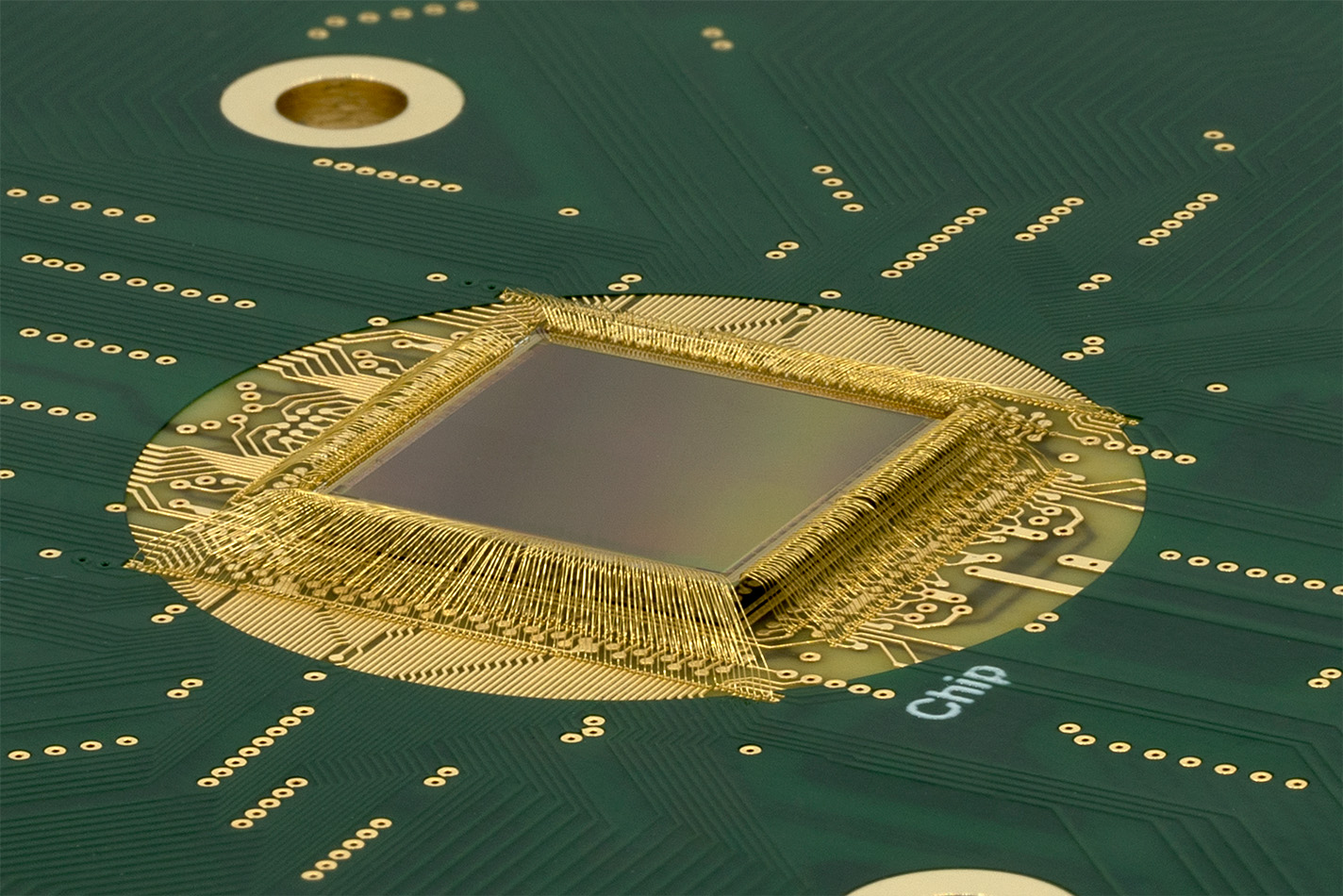
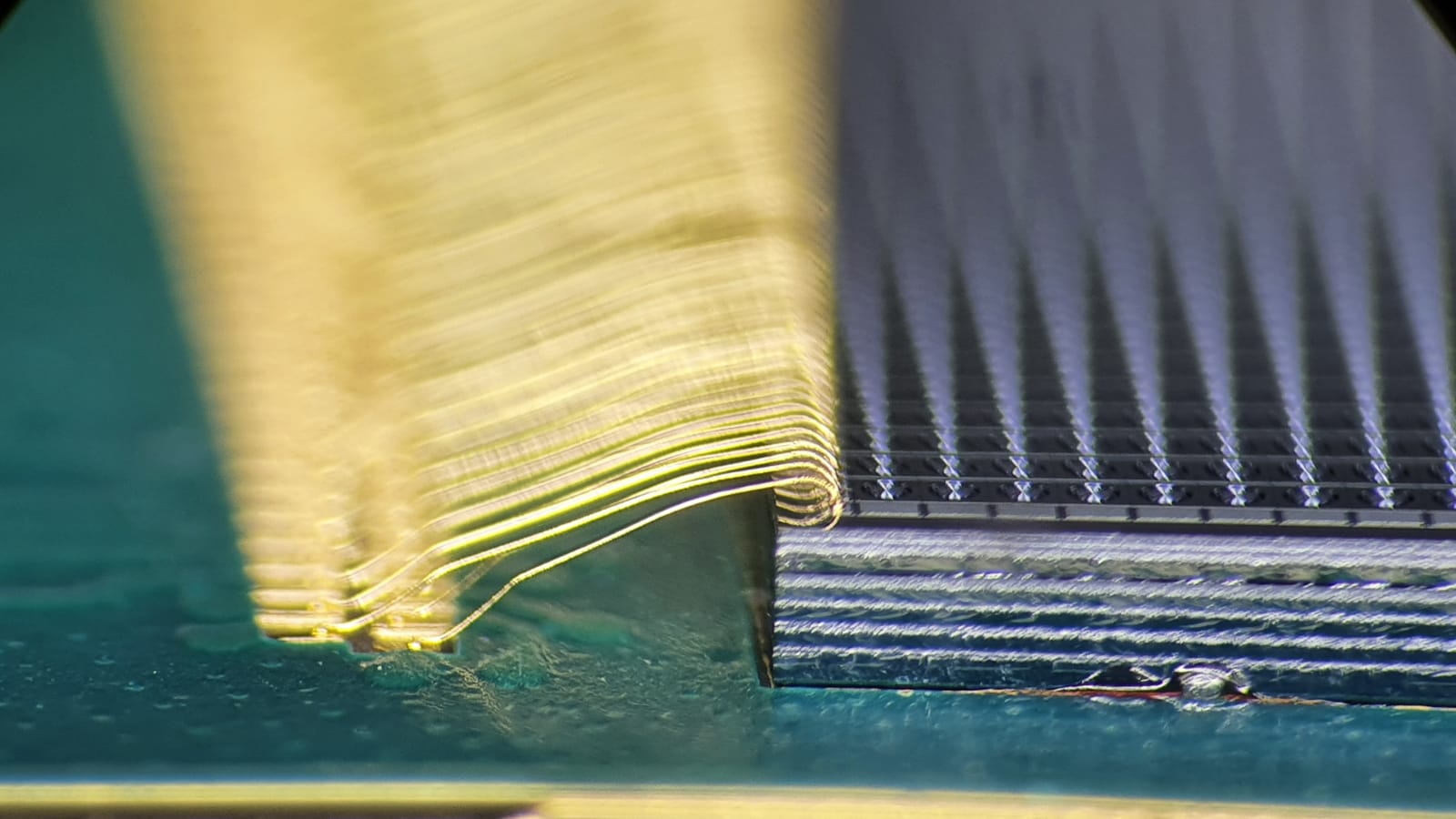
Beckermus Technologies specializes in bare die assembly, Our advanced capabilities include handling ultra-miniature components, high-density interconnects, and direct die bonding to substrates or packages, Whether working with RF amplifiers, MEMS sensors, or microprocessors, with our expertise in precision wire bonding, die attach, and encapsulation, we ensure high reliability and performance tailored to demanding applications
Open cavity packages
Beckermus Technologies offers specialized open cavity packaging for bare die applications, supporting a wide range of package types, including QFN, SOIC, DFN, TOs, and fully customized designs. whether you need Open-molded Plastic Packages (OmPP)®, Open-cavity Plastic Packages (OCPP), ceramic and plastic IC packages, organic substrates, or custom IC package configurations, tailoring each solution to meet the specific requirements of your application. Our open cavity packaging ensures precise bare die integration, excellent thermal and electrical performance, and robust reliability
COB
Our Chip-on-Board (COB) services provide a comprehensive solution for high-density, high-performance applications. Utilizing advanced assembly techniques, we directly attach bare dies to a variety of substrates including FR4, Ceramic, Flex, silicon, glass & diamond
2.5D\3D
Our 2.5D and 3D packaging services offer cutting-edge solutions for high-performance, space-saving designs in advanced electronics. Leveraging technologies such as interposers, through-silicon vias (TSVs), and stacked die integration, we enable superior functionality and performance in compact form factors. From design and prototyping to full-scale production, our 2.5D and 3D packaging solutions are programmed to meet the needs of industries requiring innovation, efficiency, and reliability.
SIP
Our System-in-Package (SiP) solutions deliver exceptional integration and performance, combining multiple ICs, passive components, and sensors into a single compact package. We specialize in designing and manufacturing SiP solutions tailored for applications demanding miniaturization and multi-functionality, including IoT, wearable devices, medical electronics, and telecommunications. With our proven expertise in advanced packaging, we ensure reliable and efficient packaging for complex systems.
Wafer dicing
By utilizing advanced equipment and processes, we deliver clean, accurate cuts on wafers of various materials, including silicon, glass, GaAs, and more. Our capabilities support dicing for wafers with ultra-thin profiles, high-density patterns, and complex geometries. Whether your needs involve small prototype batches or large-scale production, we ensure minimal chipping and debris, preserving the integrity of your delicate devices. With expertise in handling bare dies and supporting next-generation applications, our wafer dicing services are a vital step in achieving your packaging and assembly goals.