Jigs & tools
Beckermus technologies provides full in-house development of custom mechanical tooling, including jigs, fixtures, and pick-up head, specifically engineered to support the unique requirements
Read more
Beckermus Technologies offers comprehensive printed circuit board (PCB) design services tailored to the evolving needs of cutting-edge technologies across multiple domains. Our expertise spans the development of multi-layer, rigid, flex, and rigid-flex PCBs, engineered for high reliability, precision, and seamless manufacturability.
We specialize in high-density interconnect (HDI) layouts, supporting complex circuit architectures with fine-line routing, microvias, blind/buried vias, and component miniaturization. This makes our designs ideal for integration in microelectronics, RF systems, MEMS devices, and hybrid flexible electronics—where space, performance, and cross-domain functionality are critical.
We integrate thermal management directly into our design process using advanced techniques such as thermal vias, heat spreaders, and copper pours.
Our design flow includes close collaboration with customers to ensure full compatibility with their electrical, mechanical, and optical assemblies, while also complying with rigorous industry standards for reliability, EMI/EMC performance, and testing.
Whether you’re developing a precision photonics platform, a high-frequency RF module, or a flexible hybrid device, Beckermus delivers intelligent PCB design solutions built for complexity, integration, and performance.
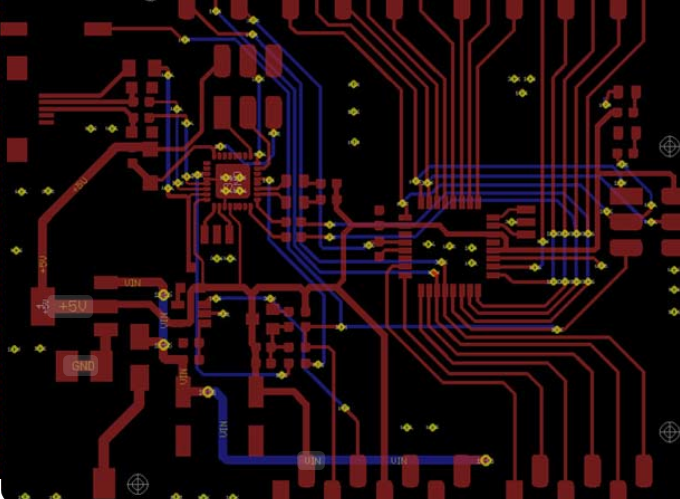
Beckermus Technologies offers comprehensive printed circuit board (PCB) design services tailored to the evolving needs of cutting-edge technologies across multiple domains. Our expertise spans the development of multi-layer, rigid, flex, and rigid-flex PCBs, engineered for high reliability, precision, and seamless manufacturability.
We specialize in high-density interconnect (HDI) layouts, supporting complex circuit architectures with fine-line routing, microvias, blind/buried vias, and component miniaturization. This makes our designs ideal for integration in microelectronics, RF systems, MEMS devices, and hybrid flexible electronics—where space, performance, and cross-domain functionality are critical.
We integrate thermal management directly into our design process using advanced techniques such as thermal vias, heat spreaders, and copper pours.
Our design flow includes close collaboration with customers to ensure full compatibility with their electrical, mechanical, and optical assemblies, while also complying with rigorous industry standards for reliability, EMI/EMC performance, and testing.
Whether you’re developing a precision photonics platform, a high-frequency RF module, or a flexible hybrid device, Beckermus delivers intelligent PCB design solutions built for complexity, integration, and performance.

Beckermus technologies provides full in-house development of custom mechanical tooling, including jigs, fixtures, and pick-up head, specifically engineered to support the unique requirements
Read more

Beckermus Technologies specializes in designing advanced microelectronic packages that meet the demands of modern applications. From ceramic and organic packages to hybrid designs our expertise includes creating open cavity packages such
Read more

Our Design for Manufacturing (DFM) services ensure that your product is engineered for seamless, high-precision production from the outset. We analyze your design specifications alongside
Read more